Komori America CorporationKomori and Seria Corporation: Driving Innovation in Printed Electronics
Seria Corporation has been a pioneer in printed circuit board (PCB) technology for nearly five decades, delivering the trusted SERIA brand of advanced screen-printing machines. Known for their precision, durability, and environmentally conscious design, Seria’s solutions meet the highest standards in quality, cost-efficiency, and safety.
In 2014, Seria joined Komori Corporation, a global leader in printing technology. This strategic partnership has empowered both companies to expand their innovation footprint across printed electronics and semiconductor packaging.
With a dedicated U.S. office offering responsive support, Komori/Seria now provides a robust portfolio of specialized equipment designed for both high-volume production and advanced R&D environments:
Additive Manufacturing Equipment for R&D and Production
Delivering high-precision, versatile systems tailored for both research laboratories and full-scale manufacturing. These solutions enable rapid innovation and prototyping in advanced electronics and material development.
PE Gravure Offset Printing: Pioneering fine-line wiring, bump printing, and fanout technologies—offering scalable, sustainable solutions for semiconductor packaging, MicroLED displays, and other advanced applications.
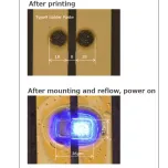
Fine & Selective Filling Printing Technology:
Supporting next-generation semiconductor and PCB manufacturing, including HDI, UHDI, and interposer production, through highly selective, precision material deposition.
High-Speed Screen-Printing Technology:
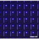
Designed for gapless alignment and high-throughput efficiency in mass production of MLCCs, RFID tags, and other high-volume electronic components.
These integrated technologies are shaping the future of printed electronics, delivering competitive advantages across automotive, consumer electronics, medical, aerospace, and IoT industries.
As part of Komori, Seria remains true to its guiding philosophy: "Kando Beyond Expectations!" Together, they are redefining what's possible in printed and additive manufacturing, enabling flexible, cost-effective, and sustainable solutions across a broad spectrum of electronic applications.