High-density mounting
Projects


Information
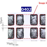
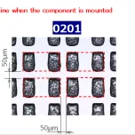
A major Japanese electronic component manufacturer has requested joint development for high-density mounting technology. Their key requirements include the ability to mount extremely small components and to minimize the spacing between adjacent parts to maximize component density on limited board space. A critical condition is avoiding solder bridging (short circuits) between neighboring solder deposits.
Component Gap: The image demonstrates a component gap as narrow as 50 µm, showcasing the precision achievable with gravure offset printing.
Solder Paste Application: Type 7 solder paste is applied to the substrate, forming microbumps that facilitate the assembly of microLEDs.
Printing Resolution: Gravure offset printing enables high-resolution printing, achieving solder bump diameters as small as 6 µm with a pitch of 30 µm.
Display Daily
MicroLED Assembly: The printed solder bumps serve as interconnects for microLEDs, which are typically 30 µm x 50 µm or 30 µm x 80 µm in size.
Display Daily
This approach addresses the challenge of assembling ultra-small components with minimal spacing, ensuring reliable connections without short circuits.
Traditional screen printing poses challenges due to limitations in printing precision and ink bleeding, making it difficult to reduce spacing between components. In response, Komori-Seria is currently testing how tightly component gaps can be reduced using gravure offset printing, which offers higher resolution and accuracy.
Recent trials using Type 7 solder paste have aimed for component spacing as narrow as 50 µm. The project is now progressing to the stage where actual component mounting is being prepared based on these print tests.
